Product Center



Product Center
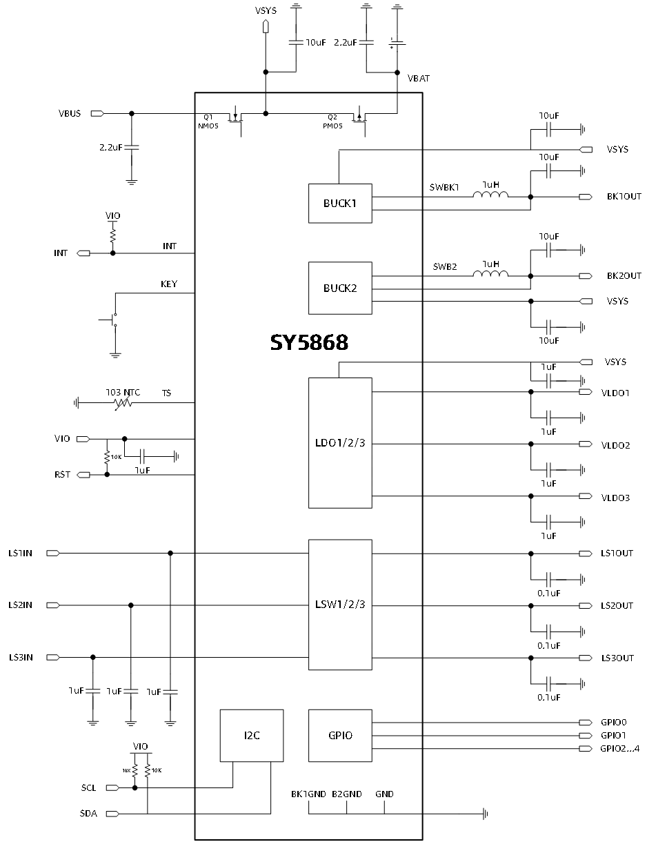
SY5868 is a highly integrated battery management unit primarily designed for ultra-low-power wearable devices. It integrates the most commonly used functions for wearable applications: a linear NVDC charger with power path management, two step-down switching converters (BUCK1 and BUCK2, where BUCK2 can be configured as BOOST), three LDO regulators (LDO1 can be configured as Always-on), three load switches (LSW1 Reconfigurable as LDO), and seven multifunctional general-purpose input/output (GPIO) ports.
The charging process of SY5868 includes pre-charge, constant-current (CC) charging, and constant-voltage (CV) regulation. The charging current and termination current are programmable via the I2C interface.
The charging cycle operates automatically. During all charging phases, the internal control loop monitors the IC junction temperature and reduces the charging current
if the internal temperature threshold is exceeded.
In addition, input over-voltage protection (OVP), input under-voltage lockout (UVLO), and input current limiting protection are integrated to provide robust input source monitoring.
The BUCK converters of SY5868 adopt the ACOT architecture to achieve fast transient response and support dynamic voltage scaling (DVS) for rapid multi-level voltage switching. The BUCK, LDO, load switch (LSW), and GPIO all support timing control to meet various power-up sequence requirements.
Standby power consumption: less than 4.5 μA (BUCK1 enabled), less than 3 μA (all power outputs disabled)
Shipmode power consumption: less than 0.5 μA, supports wake-up via key press or 5V insertion
OFF mode: Iq < 1.5 μA, supports I2C communication
Integrated NVDC power path management linear battery charger:Input voltage operating range: 3.5V to 5.5V;VBUS input voltage withstand: 28 V;Configurable battery charging voltage: ±0.5% accuracy,4 V to 4.35 V with 50 mV step; 4.35 V to 4.65 V with 10 mV step;Configurable fast charging current: 8 mA to 1 A;BATFET on-resistance: 80 mΩ;Discharge current: up to 3.2 A, supporting high system load;Charge termination current: 1–31 mA, 2 mA step, default 3 mA, configurable to double;Pre-charge current: 1–31 mA, 2 mA step, default 3 mA, configurable to double;Supports IINDPM: 300 / 500 / 1200 mA / DIS, default 500 mA;Supports VINDPM: 4.2 / 4.6 / 4.7 V / DIS, default 4.6 V;BAT UVLO thresholds: 2.42 / 2.64 / 2.82 / 2.9 V, default 2.82 V;Supports charge timeout configuration;Supports thermal loop control (120 °C);Over-temperature protection: 140 °C;Supports COLD / HOT detection, enabling safe charging over full temperature range;
Integrated dual BUCK converters :Input voltage range: 2.4–5.5 V;Output voltage range:0.4–2.0 V with 12.5 mV step;0.8–3.4 V with 25 mV step;Output voltage accuracy: ±1% @ VOUT > 1.2 V; ±1.5% @ VOUT ≤ 1.2 V;Supports Dynamic Voltage Scaling (DVS), settling time 30μs (including digital response time);Ripple:< 2% @ VOUT > 1.2 V< 20 mV @ VOUT ≤ 1.2 V;Maximum output load: 1000 mA;Supports pass-through mode, power consumption < 20 μA;Fast transient response: 100 μA–200 mA @ 100 ns, VOUT = 0.7 V load step, voltage overshoot / undershoot < 40 mV;Efficiency: up to >90% efficiency at VIN=3.7V, VOUT=1.8V;Supports output discharge function, discharge resistors: 100 Ω;Switching frequency: 1.5 / 2 / 2.5 / 3 MHz, default 1.5 MHz with 1 μH inductor;Supports 4-level drive strength adjustment: 3 / 2 / 1 / 0.6 V/ns, default 1 V/ns;Light/heavy load switching threshold: ≥ 10 mA;BUCK2 can be configured as BOOST mode(Different chip versions)
BOOST:Input voltage range: 2.4–5.5 V;Output voltage range: 2.5–5.5 V, accuracy ±2%, 50 mV step, supports Dynamic Voltage Scaling (DVS), 30 μs;Maximum load capability: 600 mA @ VOUT = 5 V, VIN = 3–4.5 V;Efficiency: up to >93% efficiency at VIN=3.7V, VOUT=5V ;Transient response: <100 mV @ 0–200 mA, tr/tf < 100 ns;Supports pass-through mode and Down Mode Supports output discharge function, discharge resistor: 160 Ω
LDO:Input voltage range: 2.4–5.5 V;Output voltage range: 0.8–3.3 V, accuracy ±2%, 50 mV step;Load capability: >300 mA;Dropout voltage: <200 mV @ 300 mA VOUT = 3.3 V, 0–60 mA, tr/tf < 1 μs,overshoot/undershoot < 100 mV;PSRR > 70 dB @ 1 kHz, VOUT = 1.8 V, @ VOUT = 3.3 V, IOUT = 50 mA;Noise: 100 μVrms @ 0.8 V, 10 mA, 10–100 kHz;Supports output discharge function, discharge resistor: 100 Ω;LDO1 supports always-on (AON)configuration (1 μA), 1.2–3.3 V, 0.1 V step, load capability: 1 mA
Load Switch (LSW):Input voltage range: 0.4–5.5 V;RON < 120 mΩ;Fast output discharge QOD, Rdis=100Ω;Over-current protection (OCP) and reverse current protection (RCP);LSW1 supports configuration as LDO mode: input voltage range 1.6–5.5 V, output voltage 0.4–3.3 V, 50 mV step;LSW1 LDO mode PSRR > 70 dB @ 1 kHz in LDO mode, 0.7 V, 10 mA output;Load capability in LDO mode: > 300 mA
Integrated fault protection for enhanced safety :Input supply current limit and over-voltage protection (OVP);Battery under-voltage, over-voltage and over-current protection;Power rail (BUCK/LDO) output under-voltage protection, over-current protection; LSW output over-current protection and reverse current protection;Thermal regulation and thermal shutdown protection;Reset mechanisms, including power-on reset, watchdog reset, key reset, register reset, and VBUS reset
Package: WLCSP36 2.52×2.41mm, 0.4 mm pitch
Wearable Devices
Smart Watch / Smart Band
邮箱:sales@tkplusemi.com
网址:www.tkplusemi.com
地址:深圳市南山区科苑南路3176号彩讯科技大厦19楼

 SY5868